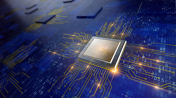
Centre nods program to develop semiconductors in India

IICA & CMAI Ink MoU to Boost India's Carbon Markets & Decarbonisation
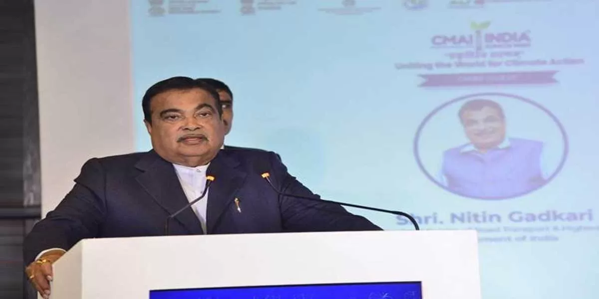
In a major step toward strengthening India’s carbon markets and advancing decarbonisation efforts, the Indian Institute of Corporate Affairs (IICA) and the Carbon Market Association of India (CMAI) formalized their collaboration through a Memorandum of Understanding (MoU) in New Delhi. The agreement was announced during the IICA-CMAI Masterclass on Global & Indian Carbon Markets, held as part of India Climate Week. The event was attended by key government officials, including the Union Minister for Road, Transport & Highways, who emphasized the importance of biofuels and green hydrogen in sh..
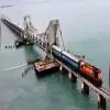
Kavach Installation on Mumbai-Delhi-Kolkata Route Extended to Dec ’25
The Railway Board has extended the deadline for the installation of the Automatic Train Protection (ATP) system, Kavach, on the Delhi-Mumbai and Delhi-Kolkata routes from March to December 2025. According to the revised railway budget estimates for 2025-26, track-side equipment for Kavach Version 4.0 will be installed across the 3,000 km stretch by the end of 2025, with work progressing on the remaining sections. Indian Railways adopted Kavach as the national ATP system in 2020, with the latest specification for Version 4.0 approved in July 2024. The project includes the installation of Kava..
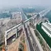
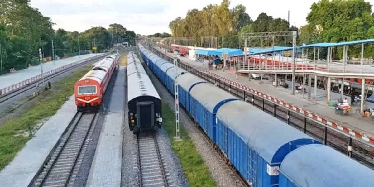
CRS Inspects Newly Doubled Nawada-Tilaiya Rail Section in ECR
The Commissioner of Railway Safety (CRS), Eastern Circle, Kolkata, Suvomoy Mitra conducted an inspection of the newly doubled Nawada-Tilaiya section under the Kiul-Gaya doubling project in Danapur Division. The inspection included a thorough assessment of the newly constructed double line and bridges in the section. As part of the evaluation, a speed trial was successfully carried out at 120 km/h using a special train between Nawada and Tilaiya. The inspection was attended by the Divisional Railway Manager (DRM) of Danapur Division, Jayant Kumar Choudhary, along with senior officials from the..
Latest Updates