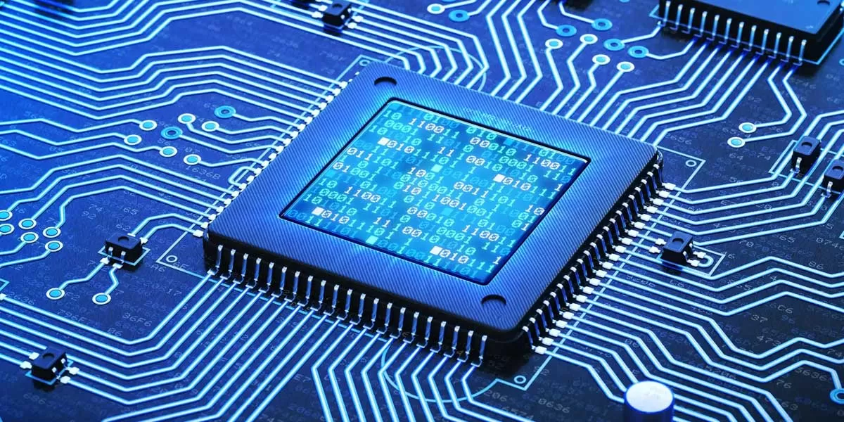
India Boosts Semiconductor Talent with Singapore Partnership
AI-Enabled Workflows Lift Profitability and Productivity
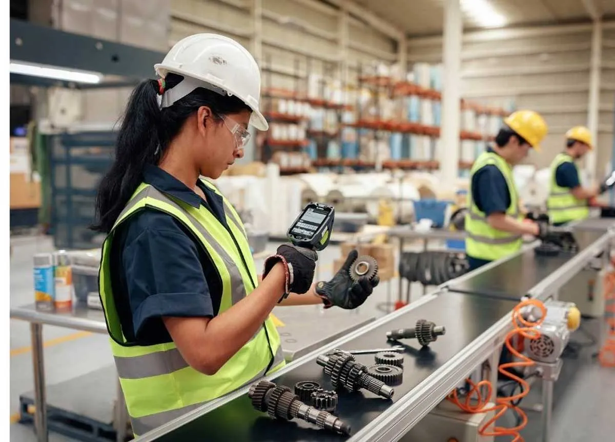
Organisations modernising frontline workflows with artificial intelligence, automation and real-time data are reporting stronger financial performance, higher productivity and improved employee engagement, according to a global study by Zebra Technologies and Oxford Economics.The research covered 1,000 senior leaders across retail, manufacturing, transportation and logistics in the US, Mexico, the UK, Germany, India, Japan, Australia and New Zealand.In transportation and logistics, 54 per cent of companies that improved picking and packing operations reported faster operational performance, wh..
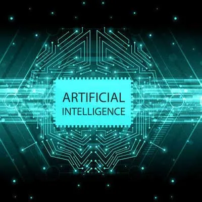
India Leads Global AI Readiness but Implementation Lags
Indian companies lead global averages across all eight artificial intelligence readiness indicators tracked by JLL, but only 19 per cent have started making changes to their workplaces, according to the JLL 2026 Future of Work Survey.The study found that 77 per cent of Indian business leaders expect AI to change their office requirements, creating a 58-percentage-point gap between awareness and implementation. The survey covered more than 2,200 CEOs, CFOs and real estate leaders across 21 countries during the first quarter of 2026.Despite concerns over automation, 58 per cent of Indian leaders..
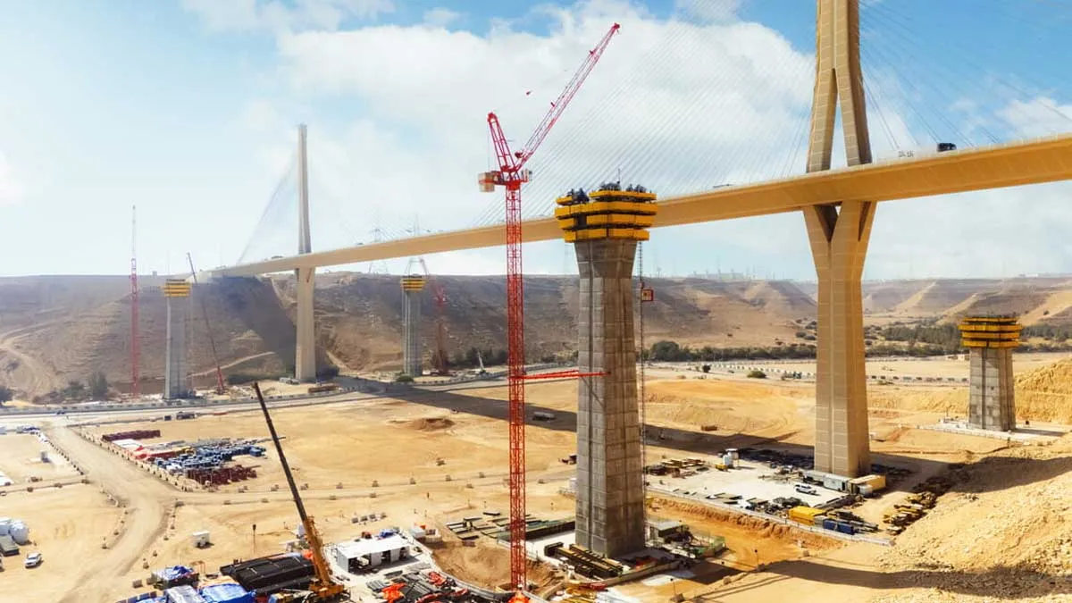
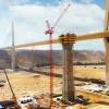
Three WOLFF Cranes Build Riyadh Cable-Stayed Bridges
Three WOLFF 180 B luffing jib cranes are supporting the construction of two cable-stayed bridges alongside the existing Wadi Laban Bridge in Riyadh, Saudi Arabia. The project is being developed for the Royal Commission for Riyadh City and executed by the ICRC joint venture comprising IC Ictas and Al Rashid Trading & Contracting Company.The cranes are handling lifting operations including formwork, reinforcement, concrete placement, work platforms, surveying equipment and other construction materials. Each crane is fitted with a 40 m jib, reaches a hook height of 157 m and offers a maximum ..
Latest Updates